Detailed Laboratory Skills, Techniques, and Knowledge acquired
Engineering Labs
ITI 1121 - Introduction to Computing II
Lab 1: Introduction to Java
Java Programming Fundamentals: Mastered core Java programming concepts including syntax, data types, variables, and basic operations for software development applications.
Error Debugging and Resolution: Developed proficiency in identifying, analyzing, and resolving compilation and runtime errors through systematic debugging techniques.
Program Development Skills: Gained expertise in creating simple Java programs from conception to execution, implementing basic algorithmic solutions and control structures.
Lab 2: Data Type Conversion/Object-Oriented Programming
Data Type Conversion Mastery: Acquired comprehensive understanding of explicit and implicit data type conversions, managing type casting accuracy and potential data loss scenarios.
Object-Oriented Design Implementation: Developed skills in creating and implementing simple classes with proper encapsulation, understanding fundamental OOP principles and design patterns.
Class Association Architecture: Mastered techniques for establishing relationships between classes, implementing inter-class communication and dependency management in complex software systems.
Lab 3: Arrays, OOP, Testing, and Documentation
Array Manipulation and References: Gained proficiency in advanced array operations, memory management, and reference handling for efficient data structure implementation.
Unit Testing Implementation: Developed expertise in creating comprehensive unit tests for Java applications, ensuring code reliability and implementing test-driven development practices.
JavaDoc Documentation Standards: Mastered professional code documentation techniques
using JavaDoc specifications, generating comprehensive web-based API documentation
for software projects.
Lab 4: Inheritance and Introduction to Interfaces
Inheritance Design Patterns: Acquired expertise in applying inheritance concepts to create scalable application architectures, implementing parent-child class relationships and method overriding.
Interface Implementation Strategy: Developed skills in designing and implementing Java interfaces, creating flexible and modular software components with standardized method contracts.
Lab 5: Classes and Interfaces
Parametrized Interface Development: Mastered implementation of generic interfaces with type parameters, creating reusable and type-safe software components for complex applications.
Comparator Interface Utilization: Gained proficiency in using java.util.Comparator for custom object sorting and comparison operations in data structure manipulation.
Abstract Class Architecture: Developed expertise in creating and implementing abstract classes, understanding the balance between concrete implementation and interface abstraction in object-oriented design.
Lab 6: Stacks, Postfix Expressions, and Data Structures
Stack Algorithm Design: Mastered recognition and implementation of stack-based algorithms, understanding LIFO principles and their application in algorithmic problem-solving scenarios.
Dynamic Array Stack Implementation: Developed proficiency in implementing stack data structures using dynamic arrays, managing memory allocation, and resizing operations for optimal performance.
Generic Type Implementation: Gained expertise in applying generic type concepts for creating type-safe, reusable data structure implementations with predefined interface specifications.
Lab 7: Exceptions and Error Handling in Java
Exception Classification Mastery: Acquired a comprehensive understanding of checked versus unchecked exceptions, implementing appropriate exception handling strategies for robust application development.
Exception Control Flow Management: Developed expertise in using try-catch-finallythrow-throws keywords for comprehensive error handling and resource management in Java applications.
Custom Exception Development: Mastered creation and implementation of custom exception classes, extending existing data structure implementations with sophisticated error handling mechanisms.
Lab 8: Queues and their Applications
Queue Algorithm Implementation: Gained proficiency in queue-based algorithms and FIFO data structure principles, understanding their applications in various computational scenarios.
Queue Data Structure Mastery: Developed expertise in implementing queues using both array-based and linked list approaches, comparing performance characteristics and memory management strategies.
Lab 9: User Input and I/O Operations
File I/O System Design: Mastered designing Java programs for reading data from keyboard input and text files, implementing robust input validation, and data processing workflows.
Output Management Systems: Developed proficiency in creating programs for writing data to console output and text files, managing file operations, and data formatting
requirements.
Exception Handling Integration: Gained expertise in modifying existing Java programs to incorporate comprehensive exception declaration and handling for I/O operations and data processing scenarios.
Lab 10: Linked Lists/Version Control
Linked List Implementation: Developed doubly linked lists with dummy nodes and enhanced existing implementations through method additions and interface integration.
Git Version Control Proficiency: Mastered essential Git commands including git, init, git add, git commit, git push, git pull, and GitHub integration for collaborative
software development.
Lab 11: Iterators and Binary-Search Trees
Iterator Design Pattern Application: Gained expertise in iterator principles and implemented iterator-based solutions for efficient data structure traversal and manipulation.
Binary Search Tree Algorithm Development: Designed and implemented recursive methods for binary search tree operations, demonstrating advanced algorithmic problem-solving skills.
ITI 1100 - Digital Systems
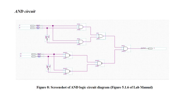
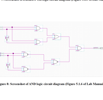
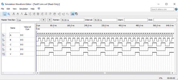
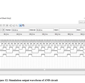
Lab 1: Logic Gates
Schematic Construction: Learned to construct combinational logic circuits from schematics
using Quartus II, including one-chip, two-chip, and three-chip configurations.
Truth Table Analysis: Gained proficiency in deriving and experimentally verifying truth tables for logic circuits to confirm their functional operation.
Logic Gate Identification: Developed skills in identifying equivalent logic gates (e.g., 3-input NAND) from circuit configurations by analyzing truth tables.
Quartus II Workflow: Mastered creating projects, drawing schematics, compiling, simulating,
and assigning pins in Quartus II 13.0 Service-Pack 1.
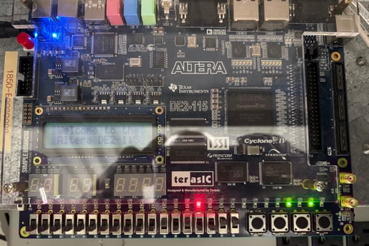
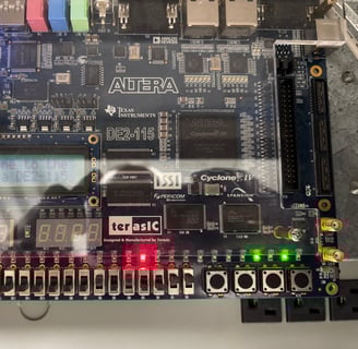
Altera DE2-115 Usage: Acquired experience in uploading compiled circuits to the Altera DE2-115 board and testing them using switches and LEDs.
Circuit Analysis: Learned to predict circuit behavior by analyzing gate outputs for all input combinations, constructing detailed truth tables.
Boolean Expressions: Gained expertise in writing Boolean logic expressions for given circuits and verifying them experimentally.
Simulation Techniques: Developed skills in creating simulation waveforms in Quartus II to verify circuit functionality before hardware testing.
Documentation: Improved ability to document experimental procedures, data, and results in a lab report, including theoretical and experimental truth tables.
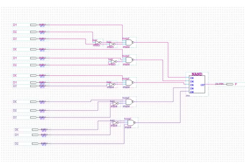
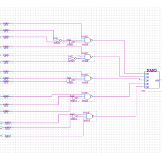
Lab 2: Boolean Logic
Boolean Simplification: Learned to simplify Boolean expressions using Boolean algebra rules and the Karnaugh map method for sum-of-products (SOP) and product-of-sums (POS) forms.
NAND Gate Implementation: Gained proficiency in implementing minimized logic functions using only NAND gates, applying De Morgan’s theorems.
Truth Table Derivation: Developed skills in deriving truth tables from Boolean expressions and verifying them experimentally on the DE2-115 board.
Circuit Minimization: Mastered minimizing combinational circuits to reduce gate count while maintaining functionality, comparing SOP and POS implementations.
Prime Number Detector Design: Learned to design a combinational circuit to detect prime numbers (0–15) using truth tables, Karnaugh maps, and NAND gates.
Quartus II Design: Enhanced expertise in creating, simulating, and testing logic circuits in Quartus II, including pin assignments for switches and LEDs.
Experimental Verification: Gained experience in experimentally verifying circuit equivalence by comparing truth tables of minimized and original circuits.
Logic Circuit Synthesis: Developed skills in synthesizing combinational circuits from functional specifications, such as prime number detection.
Report Writing: Improved documentation skills by preparing lab reports with theoretical derivations, experimental data, and circuit comparisons.
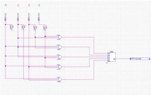
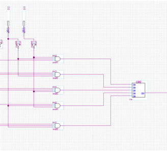
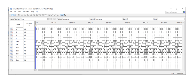
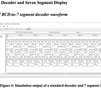
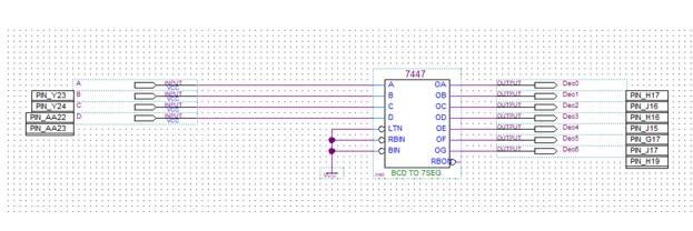
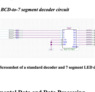
Lab 3: Decoders, Displays, and Multiplexers
Decoder Design: Learned to analyze, construct, and test a 2-to-4 decoder circuit, verifying its operation with truth tables.
7-Segment Display: Gained proficiency in using the 7447 BCD-to-7-segment decoder chip to drive a 7-segment LED display for decimal digits 0–9.
Multiplexer Analysis: Developed skills in analyzing and constructing a 4-to-1 multiplexer, determining its Boolean expression and truth table.
Quartus II Implementation: Mastered creating schematics for decoders, multiplexers, and 7-segment displays in Quartus II, including proper pin assignments.
Experimental Testing: Acquired experience in experimentally verifying circuit outputs on the DE2-115 board, comparing results with theoretical truth tables.
Pin Configuration: Learned to assign specific pins for 7-segment display segments and multiplexer inputs/outputs using the DE2-115 pin assignment tables.
Truth Table Verification: Gained expertise in constructing and verifying truth tables for multiplexers, using don’t-care terms for select inputs.
Circuit Simulation: Enhanced simulation skills in Quartus II to predict decoder and multiplexer behavior before hardware implementation.
Lab Reporting: Improved ability to document circuit designs, experimental data, and comparisons with theoretical expectations in lab reports.
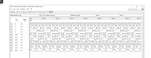
Lab 4: Arithmetic Circuits
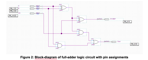
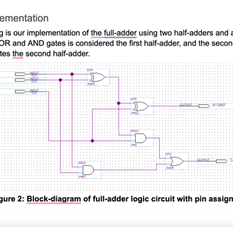
Full Adder Design: Learned to create, simulate, and test a full adder circuit, verifying its truth table experimentally on the DE2-115 board.
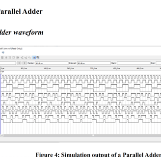
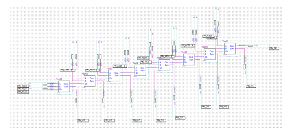
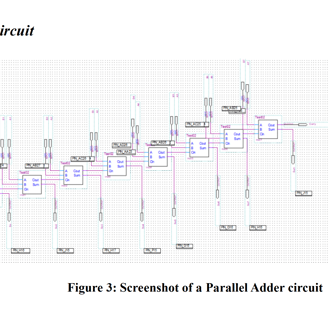
8-Bit Parallel Adder: Gained proficiency in designing an 8-bit parallel adder using full adder blocks, testing addition with binary and hexadecimal inputs.
Two’s Complement Adder/Subtractor: Developed skills in modifying an 8-bit adder to perform two’s complement addition and subtraction, including a control input (SUB).
Overflow Detection: Mastered designing an overflow detector for two’s complement arithmetic, identifying sign-bit overflow conditions.
Hierarchical Design: Learned to create hierarchical designs in Quartus II, using full adder blocks and 7-segment decoders as components.
Circuit Simulation: Enhanced expertise in simulating arithmetic circuits in Quartus II, comparing results with expected binary and hexadecimal outputs.
Pin Assignment: Gained experience in assigning pins for inputs, outputs, carry, and overflow signals on the DE2-115 board, ensuring correct LED ordering.
Arithmetic Concepts: Understood binary arithmetic, including carry propagation, two’s complement representation, and overflow in signed numbers.
Report Documentation: Improved skills in documenting arithmetic circuit designs, experimental results, and comparisons with theoretical predictions.
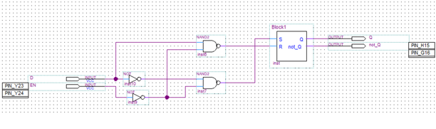
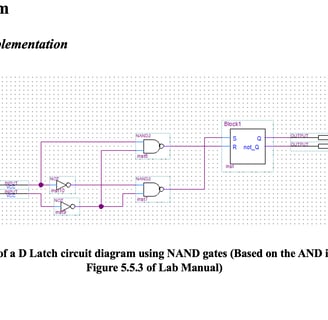
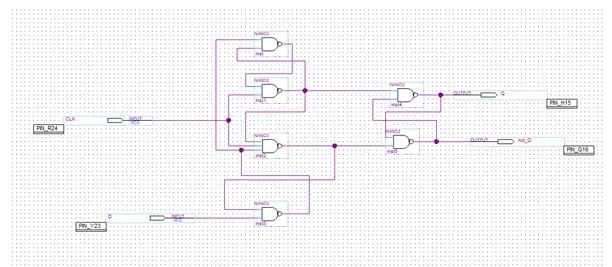
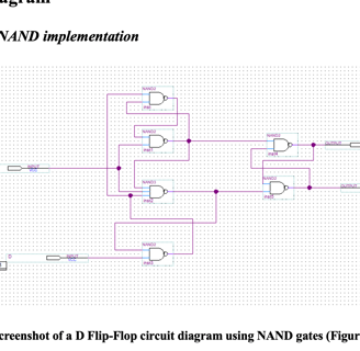
Lab 5: Latches and Flip-Flops
SR Latch Construction: Learned to build and test an SR latch using NAND gates, verifying its function table and stable states (SET, RESET).
D Latch Implementation: Gained proficiency in constructing a D latch from an SR latch, testing its behavior with ENABLE and DATA inputs.
D Flip-Flop Design: Developed skills in designing a positive edge-triggered D flip-flop, experimentally determining its triggering edge using a push button.
T Flip-Flop Creation: Mastered constructing a T flip-flop from a D flip-flop, verifying its toggle behavior with clock pulses.
Sequential Circuit Concepts: Understood the differences between latches (level-sensitive) and flip-flops (edge-sensitive), including latching and edge-triggering.
Quartus II Workflow: Enhanced expertise in creating sequential circuit schematics, simulating, and assigning pins (e.g., CLK to push buttons) in Quartus II.
Experimental Verification: Gained experience in experimentally determining function and excitation tables for latches and flip-flops on the DE2-115 board.
Negative Logic Handling: Learned to account for negative logic in DE2-115 push buttons when testing clock inputs for flip-flops.
Lab Reporting: Improved documentation of sequential circuit behavior, experimental procedures, and comparisons with theoretical function tables.
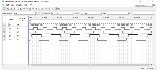
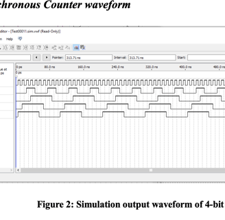
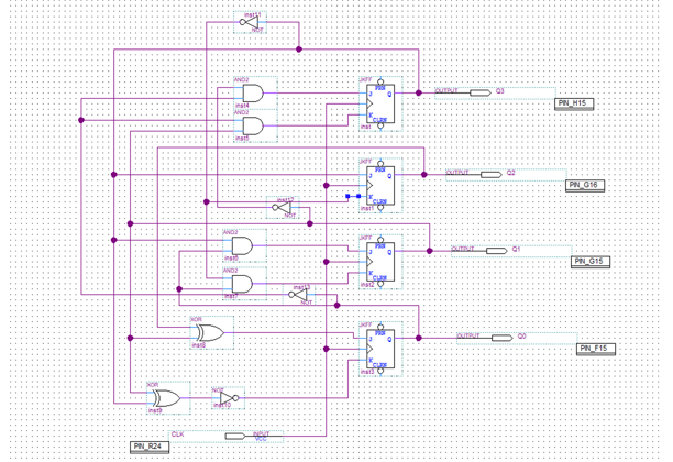
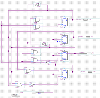
Lab 6: Synchronous Counters
Synchronous Counter Design: Learned to design synchronous counters using JK flip-flops, starting from state diagrams and deriving state tables.
Karnaugh Map Application: Gained proficiency in using Karnaugh maps to derive flip-flop input equations, handling don’t-care and unused states.
Counter Implementation: Developed skills in implementing synchronous counters in Quartus II, connecting flip-flops and combinational logic.
Counter Simulation: Mastered simulating counter sequences in Quartus II, verifying state transitions against the specified count sequence.
Experimental Testing: Gained experience in testing synchronous counters on the DE2-115 board, using push buttons for clock input and LEDs for output display.
State Diagram Analysis: Understood how to interpret state diagrams to specify count sequences and derive flip-flop inputs for counter design.
Pin Assignment: Learned to assign pins for flip-flop outputs and clock inputs, ensuring correct mapping to DE2-115 LEDs and push buttons.
Sequential Logic Principles: Enhanced knowledge of synchronous sequential circuits, including state transitions and flip-flop excitation tables.
Report Documentation: Improved ability to document counter designs, state tables, experimental count sequences, and comparisons with state diagrams.
CEG 2136 - Computer Architecture I
Lab 1: Introduction to Quartus II Design Software
Quartus II Environment: Gained familiarity with the Altera Quartus II 13.0sp1 software, including project creation, file management, and navigation of the user interface.
Schematic Design: Learned to capture logic circuit schematics using the Quartus II Graphic Editor, including placing and connecting logic gates (AND, OR, XOR) and input/output pins.
Full Adder Implementation: Developed skills in designing a simple full adder circuit with inputs A, B, Cin and outputs S (sum) and Cout (carry-out), deriving its logic
equations and truth table.
Compilation Process: Mastered compiling projects in Quartus II, troubleshooting errors, and understanding the compilation workflow, including saving and recompiling after changes.
Simulation Techniques: Acquired expertise in creating waveform files (.vwf) for functional and timing simulations, generating test vectors, and analyzing simulation results to verify circuit behavior.
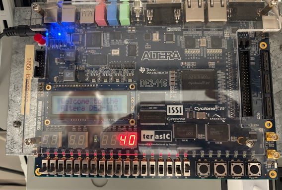
DE2-115 Board Usage: Learned to configure and program the Altera DE2-115 FPGA board, including connecting USB-Blaster, setting RUN/PROG switch, and uploading designs.
Pin Assignments: Gained proficiency in assigning FPGA pins to circuit inputs (e.g., slide switches SW0–SW2) and outputs (e.g., LEDs LEDR0–LEDR1) using the Assignment Editor.
Static Testing: Developed skills in statically testing circuits by manually applying input combinations via slide switches and observing outputs on LEDs, verifying against truth tables.
Documentation and Reporting: Improved ability to document schematics, simulation results, and experimental data in lab reports, including exporting schematics as images and personalizing output names with student numbers.
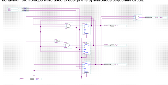
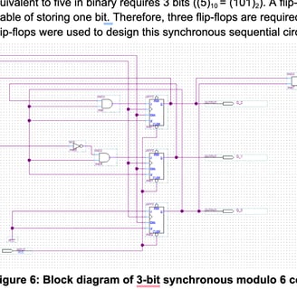
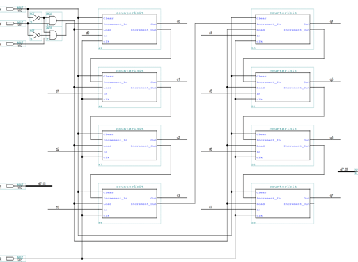
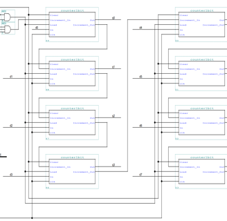
Lab 2: Design, Simulation, and Experimental Verification of Sequential Logic Circuits
Synchronous Counter Design: Learned to design synchronous modulo 6 and BCD counters using JK flip-flops, deriving state diagrams, excitation tables, and minimized Boolean expressions via Karnaugh maps.
Quartus II Schematic Capture: Gained proficiency in capturing counter schematics in Quartus II Graphic Editor, using JK flip-flops and implementing control inputs like count and reset.
Simulation Setup: Mastered creating waveform files (.vwf) in Quartus II, configuring clock signals (e.g., 20 ns period), control inputs, and bus representations to simulate counter behavior.
Pin Assignments: Developed skills in assigning FPGA pins to counter signals (e.g., CCLK, flip-flop outputs, reset) and 7-segment display segments using the Assignment Editor or Pin Planner, referencing DE2-115 User Manual.
Manual Testing: Acquired experience in manually testing counters using push-button (KEY0) as clock input, observing outputs on LEDs and 7-segment displays, and verifying count sequences against state diagrams.
7-Segment Display Integration: Gained expertise in connecting counter outputs to a BCD-to-7-segment decoder (7446) to display decimal values on DE2-115 7-segment displays, handling active-low inputs.
Modular Design: Developed skills in creating and using counter symbols (.bsf) to design a modulo 60 counter by combining modulo 6 and BCD counters in a hierarchical schematic.
Lab Reporting: Improved documentation skills by logging procedures, capturing schematics, waveforms, and oscilloscope snapshots, and compiling comprehensive lab reports with test results.
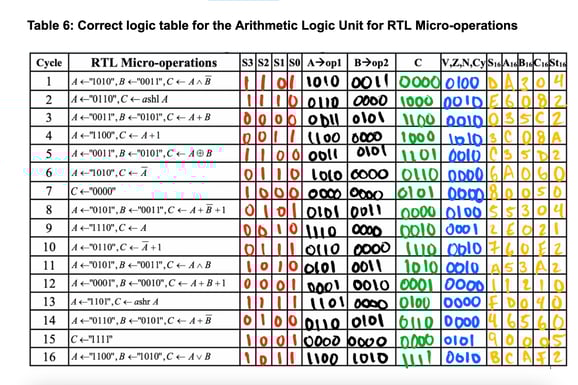
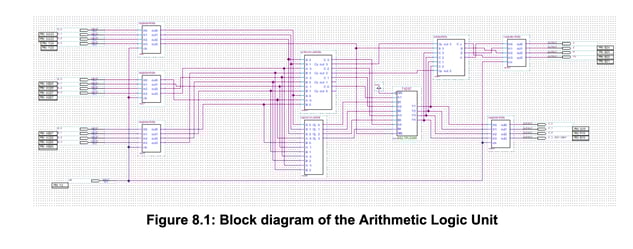
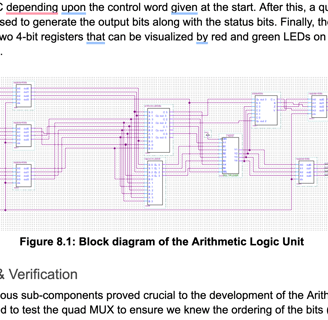
Lab 3: Arithmetic Logic Unit (ALU)
ALU Design: Learned to design a 4-bit Arithmetic Logic Unit (ALU) capable of performing 16 micro-operations (arithmetic, logic, and shift) on two 4-bit operands, as specified in a functional table.
Hierarchical Design: Gained proficiency in creating a hierarchical design structure, implementing 1-bit and 4-bit modules for Logic and Shift Circuit (LSC), Arithmetic Circuit (AC), full adder, 4-bit register, and status circuit.
Logic and Shift Circuit (LSC): Developed skills in designing a 1-bit LSC module using multiplexers (e.g., 74151 or lpm mux) to handle logic operations (AND, OR, XOR) and shifts, and scaling it to a 4-bit LSC.
Arithmetic Circuit (AC): Mastered designing a 4-bit AC using a full adder and multiplexers (e.g., 4-to-1) to perform arithmetic operations like addition, subtraction, and increment, with derived logic for carry-in.
Status Circuit: Acquired expertise in deriving and implementing logic equations for ALU status bits (Carry, Sign, Zero, Overflow) using conventional gates, based on arithmetic operation outcomes.
Quartus II Implementation: Enhanced proficiency in capturing schematics in Quartus II Graphic Editor, creating symbols (.bsf) for modules, and compiling designs for the EP4CE115F29C7 FPGA.
Simulation: Learned to create and simulate test vectors (.vwf) in Quartus II, setting clock periods (e.g., 40 ns), grouping signals, and verifying ALU outputs against a predefined micro-operation sequence.
Pin Assignments: Gained experience in assigning FPGA pins to ALU inputs (slide switches for A, B, S), outputs (LEDs for C, status bits), and clock (50 MHz oscillator)
using the Assignment Editor.
Experimental Testing: Developed skills in programming the DE2-115 board to test ALU functionality, manually applying inputs via slide switches and verifying outputs on LEDs against simulation results.
Lab Reporting: Improved documentation skills by including functional tables, schematics, simulation waveforms, compilation logs, and test results in a comprehensive lab report.
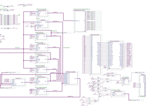
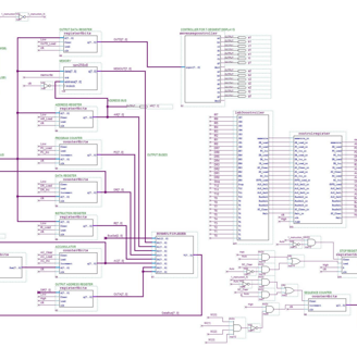
Lab 4: Basic Computer Organization - Building a Central Processing Unit (CPU)
Basic Computer Architecture: Learned the structure of a basic computer with a 256x8-bit memory, 8-bit memory-reference instructions (opcode + operand address), and
differences from the textbook model (e.g., 16-bit vs. 8-bit words).
Control Unit Design: Gained proficiency in designing a Control Unit (CU) using combinational logic (AND, OR, NOT gates) to generate control signals for the datapath,
based on RTL expressions and instruction cycles.
Instruction Decoding: Mastered deriving logic equations for control signals using Instruction Register (IR), Data Register (DR), Sequence Counter (SC), and Stop
signals, implementing direct, indirect, and register-reference instructions.
Quartus II Implementation: Enhanced skills in creating and compiling Quartus II projects, integrating provided .bdf files, designing the CU in lab3controller.bdf, and setting lab3top.bdf as the top-level entity for the DE2-115 board.
Memory Initialization: Acquired expertise in creating and editing Memory Initialization Files (.mif) to load machine code programs into 256x8-bit RAM, using hexadecimal
radix for addresses and content.
Simulation and Debugging: Developed skills in simulating the computer using .vwf files in Quartus II, setting 20 ns grid size, and debugging control signals in automatic and manual modes (using Auto signal and push-button stepping).
Pin Assignments: Learned to assign FPGA pins for clock (50 MHz), DIP switches (memory address), LEDs (AR, DR, AC, Stop), 7-segment displays (memory content),
and push-button (instruction stepping) per the provided pin table.
Machine Code Programming: Gained experience in writing and analyzing machine code programs for operations like addition, subtraction, and branching, using opcodes from a predefined instruction set and storing results in memory.
Program Analysis: Improved ability to analyze programs by tracing register and memory contents, writing pseudo-code, and understanding the role of indirect addressing in memory-reference instructions.
Lab Reporting: Strengthened documentation skills by including CU block diagrams, simulation snapshots, answers to prelab questions, and program execution results in a comprehensive lab report.
Built with Heart, Pride, and Lots of Caffeine.
If you've made it this far, then it turns out I'm less boring than I thought! Feel free to reach out by filling out the form below. Cheers!
Get in touch!
I would love to hear from you. If you have any questions, comments, or would like to work with me, please don't hesitate to reach out!